
Interview with Christian Sommer – Europe’s place in a multipolar world
“In Germany, we grew up expecting our products to last 100 years – and brands like Siemens and Miele stand for longevity. But today’s world is forcing us into much shorter cycles,” says Christian Sommer.
Interview with Christian Sommer – How do German media view China?
“Western media are always ambivalent because they are very critical and therefore often focus on negative topics,” explains Christian Sommer. Since 2005, he has been CEO & Chairman of the German Center for Industry and Trade Shanghai Co Ltd
Interview with Christian Sommer – How is Germany perceived in China?
In China, planning tends to be done on a quarterly basis, which already includes measures for implementation in the face of constantly changing global conditions Sommer has been living and working in China for more than 20 years.
Transatlantic Innovation Week 2023 – Chapter 3.5: Müzeyyen Carrasco-Demir, CEO ComSIT
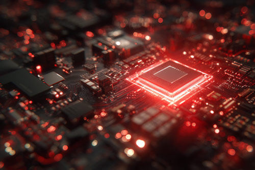
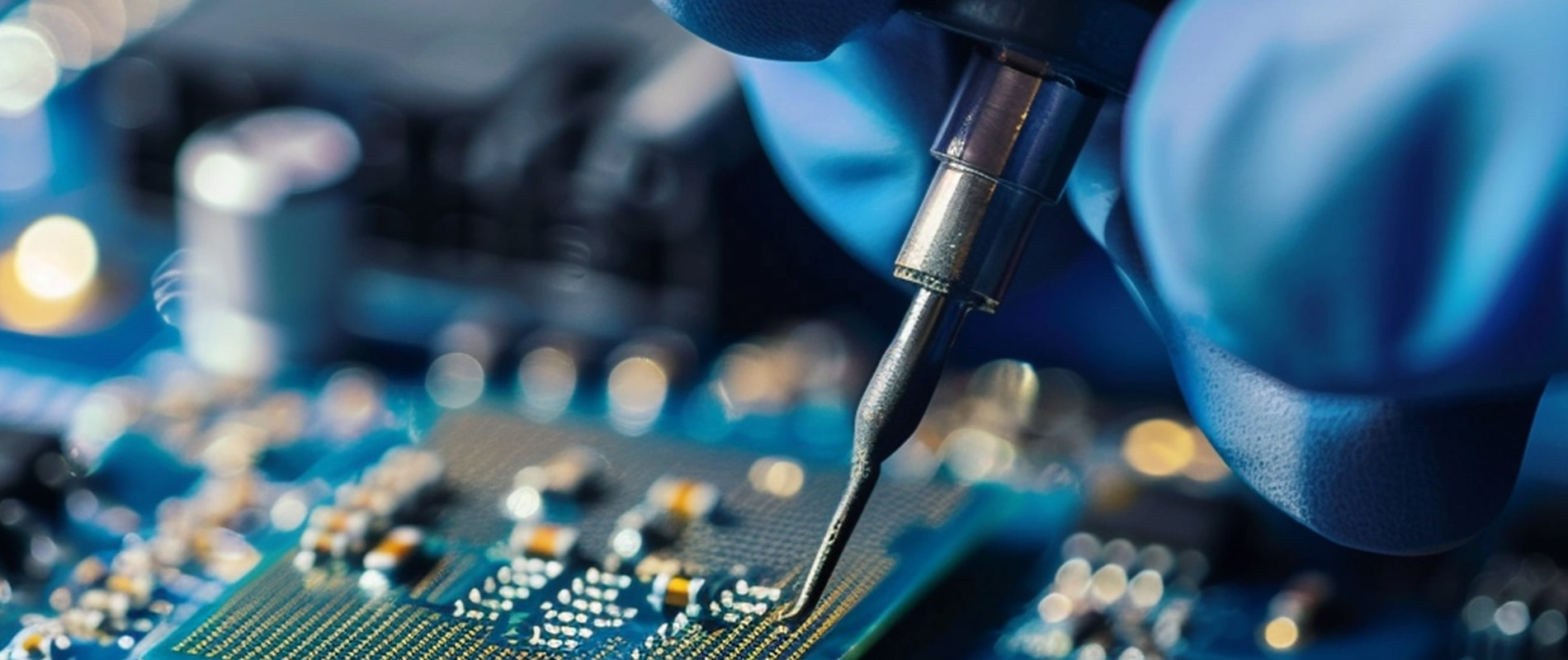
Geopolitical, social and economic challenges in the semiconductor industry how to secure the future?
#ComSit #Semiconductors